- 您现在的位置:买卖IC网 > Sheet目录325 > FAN5640S7X (Fairchild Semiconductor)IC LED DRIVER DUAL CC SC70-6
�� �
�
�Application� Information�
�Setting� the� Output� Current� Level�
�An� internally� generated� reference� current� is� mirrored� on�
�the� MOSFETs� connected� to� the� outputs� IOUT1� and�
�IOUT2� (pins� 1� and� 6,� respectively).� The� current� mirror�
�ratio� is� 275� (typical).� The� voltage� on� pin� 3� (RSET)� is�
�0.475V� in� steady� state;� therefore,� the� programmed�
�current� through� each� of� the� outputs� is:�
�External� Capacitors�
�Because� the� FAN5640� is� stable� without� capacitors� on�
�the� outputs,� no� capacitors� are� recommended.� Typical�
�input� decoupling� usually� present� on� incoming� supply�
�rails� should� suffice� in� most� applications.� If� necessary,� a�
�small� input� capacitance� may� be� placed� between� the�
�input� pin� and� ground� without� adverse� effects.�
�I� OUT� ?� 275� ?�
�0 . 475�
�R� EXT�
�EQ.� 1�
�Dropout� Limitations�
�As� for� any� LDO� regulator,� there� are� limitations� on� how�
�R� EXT� ?� 275� ?�
�?� 275� ?�
�?� 5� .� 225� k� ?�
�EQ.� 2�
�where� R� EXT� is� the� external� resistor� connected� from� pin� 3�
�to� ground.� Increasing� this� external� programming� resistor�
�reduces� the� output� current.� For� the� maximum� rated�
�25mA� rating� of� each� output,� the� minimum� value� of� the�
�external� resistor� is:�
�0 . 475 0 . 475�
�I� OUT� 0� .� 025�
�The� LED� output� current� accuracy� is� ±10%� for� 25mA�
�current� (� see� the� Electrical� Characteristics� table� ).� In� the�
�worst-case� scenario,� the� calculated� value� of� I� OUT� can�
�lead� to� an� error� of� ±10%� in� the� LED� current.� Since� the�
�tolerance� of� R� EXT� also� affects� the� LED� current� accuracy,�
�a� precision� resistor� should� be� chosen� to� have� the� least�
�effect� on� the� overall� accuracy� of� the� LED� current�
�(� see� Figure� 12� ).�
�Floating� vs.� Tied� Outputs�
�Unused� outputs� can� be� left� floating.� The� current� through� is�
�zero,� regardless� of� the� current� programmed� at� pin� 3.�
�However,� ESD� protection� is� enhanced� if� the� unused�
�output� pin� is� tied� to� VIN� (pin� 5).�
�If� the� two� output� pins� are� tied� together,� they� can� deliver�
�a� combined� 50mA� for� the� same� programming� resistor� of�
�5.225k� ?� .�
�L�
�close� the� input� and� output� rails� can� be� to� maintain�
�regulation.� The� minimum� difference� is� referred� to� as� the�
�dropout.� The� relevant� information� is� provided� in� the�
�Typical� Performance� curve� Dropout� Voltage� vs.� LED�
�Current� (� see� Figure� 8� ).� The� equation� for� the� data� is:�
�V� DO� ?� 0� .� 35� V� ?� I� OUT� ?� 64� ?� EQ.� 3�
�This� is� equivalent� to� an� R� DS� of� 64� ?� with� an� additional�
�offset� of� 350mV.� This� equation� is� helpful� in� determining�
�the� minimum� dissipation� in� the� device� and� the� lowest�
�input� voltage� for� a� given� application.�
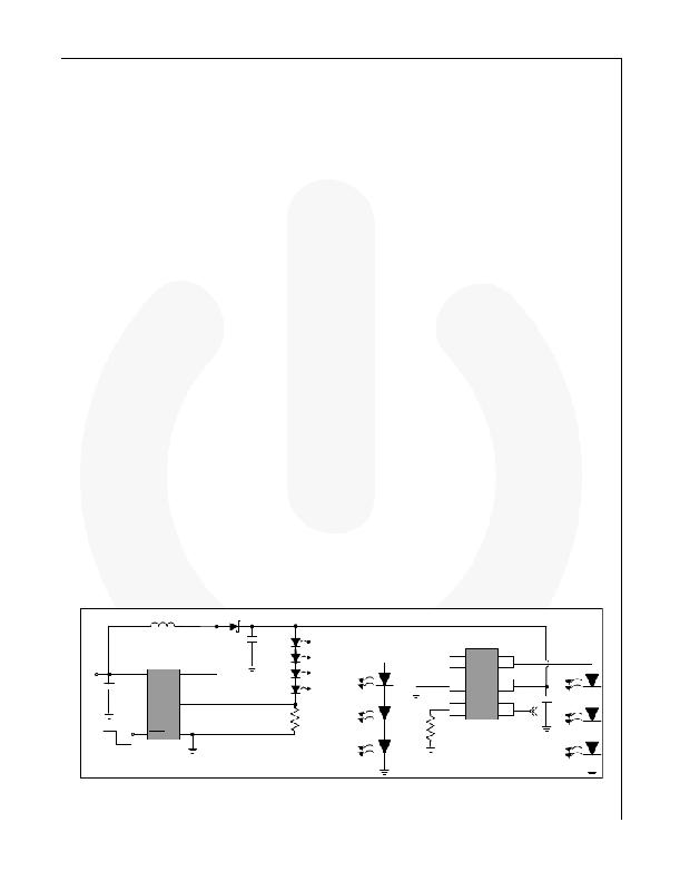
�Multiple� LED� Displays�
�For� portable� applications,� the� FAN5640� can� be� powered�
�from� the� output� of� any� typical� boost� regulator.� Multiple�
�LED� displays� can� be� created� with� the� FAN5640� powered�
�from� the� output� of� the� FAN5333,� as� shown� in� Figure� 20.�
�Note� that� the� output� voltage� of� the� FAN5333� depends�
�upon� the� number� of� LEDs� in� its� output� string.� Being�
�conscious� of� the� minimum� dropout� requirements� of� the�
�FAN5640;� if� three� series� LEDs� are� required� to� be�
�present� at� its� output,� then� the� FAN5333� should� have�
�four� series� LEDs� in� its� output� string.�
�6.8μH� to�
�10μH�
�C� OUT�
�0.1μF�
�to�
�2�
�V� IN�
�C� IN�
�4.7μF�
�to�
�10μF�
�VIN�
�SW�
�FB�
�2.2μF�
�IOUT1� 1�
�GND�
�RSET� 3�
�6� IOUT2�
�5� VIN�
�4� EN�
�ON�
�OFF�
�SHDN� GND�
�FAN5333�
�R� EXT�
�FAN5640�
�Figure� 20.� LED� Display� Example�
�?� 2006� Fairchild� Semiconductor� Corporation�
�FAN5640� ?� Rev.� 1.0.2�
�8�
�www.fairchildsemi.com�
�发布紧急采购,3分钟左右您将得到回复。
相关PDF资料
FAN5646S700X
IC LED DRIVER BLINKER SC70-5
FAN5701UMP30X
IC LED DVR MULTI 30MA 16-UMLP
FAN5702UC30X
IC LED DVR 6LED 30MA I2C 16WLCSP
FAN7080MX_GF085
IC GATE DRIVER HALF BRIDGE 8SOIC
FAN7081MX_GF085
IC GATE DRIVER HI SIDE 8-SOIC
FAN7083MX_GF085
IC GATE DVR HI SIDE RESET 8-SOIC
FAN7085M_GF085
IC GATE DVR HI SIDE 8-SOIC
FAN7171MX_F085
IC GATE DVR HIGH SIDE 8-SOIC
相关代理商/技术参数
FAN5645
制造商:FAIRCHILD 制造商全称:Fairchild Semiconductor 功能描述:Indicator LED Blinker with Single-Wire Interface
FAN5645_ABB3026B WAF
制造商:Fairchild Semiconductor Corporation 功能描述:
FAN5645MPX
功能描述:LED照明驱动器 LED W/SINGLE WIRE INTERFACE RoHS:否 制造商:STMicroelectronics 输入电压:11.5 V to 23 V 工作频率: 最大电源电流:1.7 mA 输出电流: 最大工作温度: 安装风格:SMD/SMT 封装 / 箱体:SO-16N
FAN5646
制造商:FAIRCHILD 制造商全称:Fairchild Semiconductor 功能描述:Programmable Indicator “Soft” LED Blinker with TinyWire? Single-Wire Interface
FAN5646_11
制造商:FAIRCHILD 制造商全称:Fairchild Semiconductor 功能描述:Programmable Indicator a??Softa?? LED Blinker with TinyWirea?¢ Single-Wire Interface
FAN5646S700X
功能描述:LED照明驱动器 Prog. Indicator Soft LED Blinker
RoHS:否 制造商:STMicroelectronics 输入电压:11.5 V to 23 V 工作频率: 最大电源电流:1.7 mA 输出电流: 最大工作温度: 安装风格:SMD/SMT 封装 / 箱体:SO-16N
FAN5646S700X_11
制造商:FAIRCHILD 制造商全称:Fairchild Semiconductor 功能描述:Programmable Indicator a??Softa?? LED Blinker with TinyWirea?¢ Single-Wire Interface
FAN5646S701X
功能描述:LED照明驱动器 Prog. Indicator Soft LED Blinker
RoHS:否 制造商:STMicroelectronics 输入电压:11.5 V to 23 V 工作频率: 最大电源电流:1.7 mA 输出电流: 最大工作温度: 安装风格:SMD/SMT 封装 / 箱体:SO-16N